(China (Mainland))

Product Summary
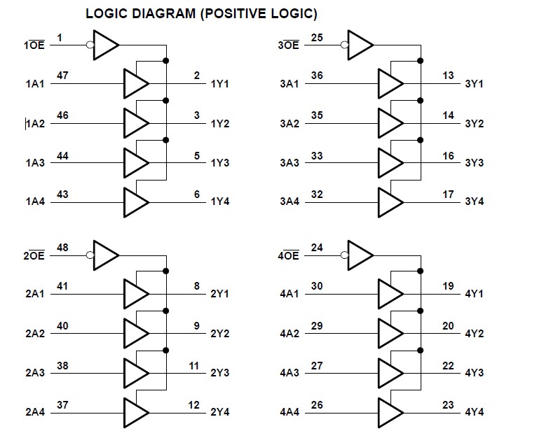
This 16-bit buffer/driver of the LVC16244A is designed for 1.65-V to 3.6-V VCC operation. The LVC16244A is designed specifically to improve the performance and density of 3-state memory address drivers, clock drivers, and bus-oriented receivers and transmitters. The LVC16244A can be used as four 4-bit buffers, two 8-bit buffers, or one 16-bit buffer. It provides true outputs and symmetrical active-low output-enable (OE) inputs. Input of the LVC16244A can be driven from either 3.3-V or 5-V devices. This feature allows the use of this device as a translator in a mixed 3.3-V/5-V system environment.
Parametrics
LVC16244A absolute maximum ratings: (1)VCC Supply voltage range: –0.5 to 6.5 V; (2)VI Input voltage range: –0.5 to 6.5 V; (3)VO Voltage range applied to any output in the high-impedance or power-off state: –0.5 to 6.5 V; (4)VO Voltage range applied to any output in the high or low state: –0.5 VCC + 0.5 V; (5)IIK Input clamp current VI < 0 –50 mA; (6)IOK Output clamp current VO < 0 –50 mA; (7)IO Continuous output current: ±50 mA.
Features
LVC16244A features: (1)Member of the Texas Instruments Widebus Family; (2)Operates From 1.65 V to 3.6 V; (3)Inputs Accept Voltages to 5.5 V; (4)Max tpd of 4.1 ns at 3.3 V; (5)Typical VOLP (Output Ground Bounce) <0.8 V at VCC = 3.3 V, TA = 25℃; (6)Typical VOHV (Output VOH Undershoot) >2 V at VCC = 3.3 V, TA = 25℃; (7)Ioff Supports Partial-Power-Down Mode Operation; (8)Supports Mixed-Mode Signal Operation on All Ports (5-V Input/Output Voltage With 3.3-V VCC); (9)Latch-Up Performance Exceeds 250 mA Per JESD 17; (10)ESD Protection Exceeds JESD 22.
Diagrams
 |
 LVC1T45MDCKREPG4 |
Texas Instruments |
Translation - Voltage Levels EP SglB Dual-Supply Bus Xcvr |
Data Sheet |
|
|
||||||||||||